19. September 2022

Launch of the Horizon Europe RIA project PATTERN

Dieser Artikel ist nur auf Englisch verfügbbar.

PATTERN will bring long-awaited breakthroughs in the field of Photonic Integrated Circuits (PICs) and provide unrivalled new functionalities for a vast range of applications. The project will devise the world’s first Process Design Kit (PDK) and Assembly Design Kit (ADK) for microwave photonics at ultra‐high frequencies above 100 GHz, new methods for heterogenous integration of III-v gain materials (e.g. InP) as well as BiCMOS drivers with electro-optic and nonlinear platform of a thin-film lithium-niobate-on-insulator (LNOI). It also develop new functionalities in PICs such as acousto-optic modulation (AOMs) and optical isolation capabilities. PATTERN’s impact will be showcased through several demonstrators, from quantum to satellite free-space communications to ultrastable optical-based RF-sources. The results of PATTERN will be accessable to the photoncis community in the form of an open access foundry.

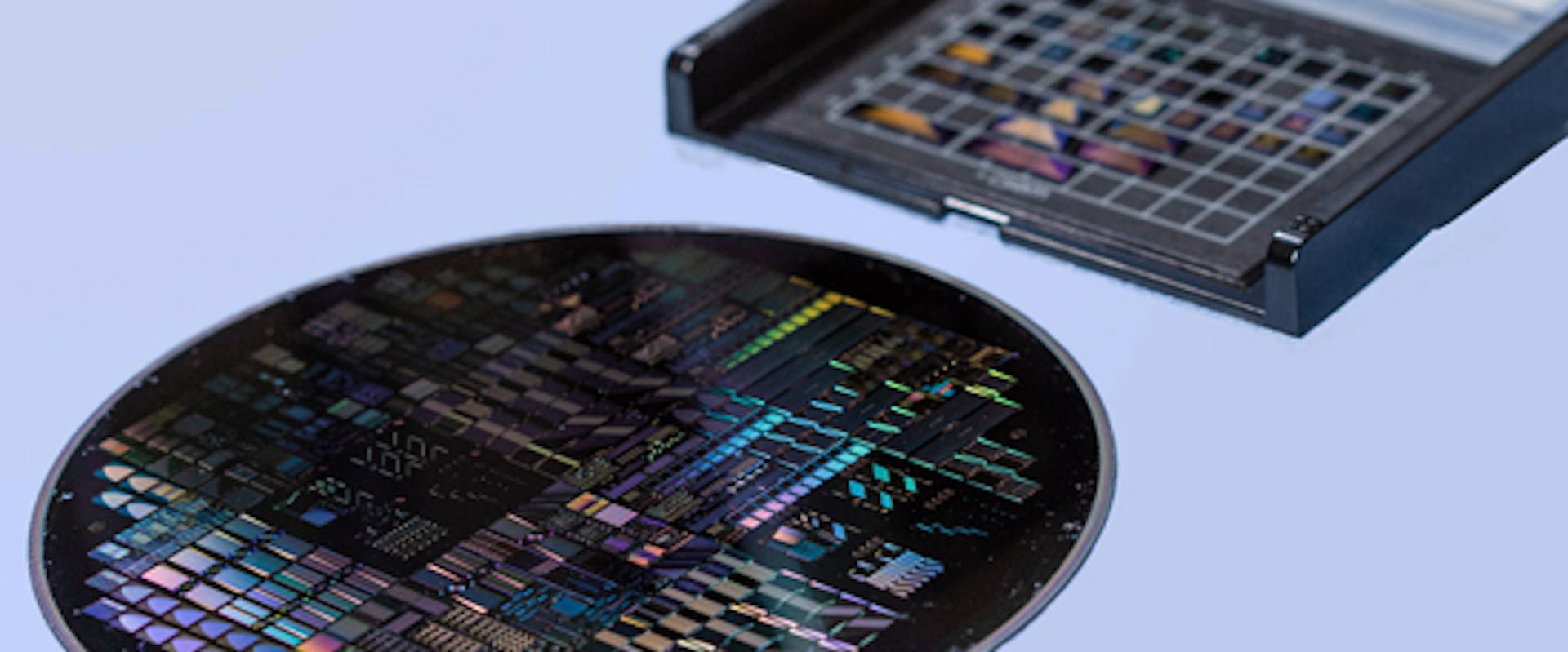
Photonic integrated circuits on a wafer

WHAT PATTERN IS ABOUT

PATTERN is an acronym for the project title “Next-generation ultra-high-speed microwave Photonic integrATed circuiTs using advancEd hybRid iNtegration”. The 48-month project started on 1 September 2022. It is funded by the European Commission under the Horizon Europe programme with a budget of 5 million euros and involves ten partners.

PATTERN aims to develop the world’s first PDK and ADK for microwave photonics at ultra-high frequencies above 100 GHz. It will introduce novel functionalities into PICs that currently do not exist, such as magneto-optic isolators and acousto-optic modulators (AOMs). PATTERN’s approach to ultra-high frequencies is holistic and includes photonic and electronic co-integration and covers all PIC foundry process steps, from design and simulation to device fabrication, packaging, and testing, including demonstration of several PIC prototypes with advanced functionalities. To this end, PATTERN will:

  • Elaborate hybrid integration solutions for various existing and emerging PIC platforms. To achieve this goal, PATTERN proposes a massive hybrid / heterogenous integration campaign between InP and LNOI platforms through methods such as butt-coupling, flip-chip bonding and micro-transfer printing, but also use of new materials such as yttrium iron garnet (YIG) to add magneto-optic functionalities to PICs. PATTERN will also develop solutions for the co-integration of electronic silicon germanium (SiGe) chips with PICs, which is a necessity especially at ultra-high speeds. In addition, PATTERN will concentrate specifically on innovative packaging solutions for such high frequencies, which are currently one of the main bottlenecks in this field.
  • Develop software expertise for design automation (e.g. RF signal routing) and end-to-end circuit simulation and design, which is extremely challenging at ultra-high frequencies.
  • Demonstrate the capabilities of the new PIC platform through prototypes for six different applications.
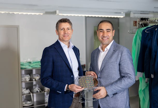
Engineer in a lab

PATTERN's approach aims to address many challenges in microwave photonics and PICs at the same time and attempts to integrate all major photonic functionalities on a single hybrid PIC: light generation, transmission, manipulation and detection, as well as electronic co-integration. PATTERN will pave the way for a new generation of advanced PICs with unrivalled novel functionalities, which will serve a wide range of applications from telecom and 5G/6G to quantum, LiDAR, optical computing and sensing technologies.
THE PARTNERSHIP

The PATTERN consortium unites the expertise of ten renowned research entities, SMEs, and industrial players in the photonics sector to achieve ambitious objectives within the project runtime of 48 months:

  • THALES SA (France)
  • Luceda Photonics (Belgium)
  • PHIX BV (The Netherlands)
  • Fraunhofer Heinrich-Hertz-Institut (Germany)
  • Interuniversity Microelectronics Centre (Belgium)
  • CNRS – Centre National de la Recherche Scientifique (France)
  • Microwave Photonics GmbH (Germany)
  • L-UP SAS (France)
  • CSEM (Switzerland)
  • University College London (United Kingdom)