Thin-Film Lithium Niobate Foundry Services by CSEM

CSEM supports the photonic community with various services based on its standardized TFLN PIC platform, dependable process design kit (PDK) and a 150 mm wafer-scale fabrication process, which includes PIC design, manufacturing, and testing.

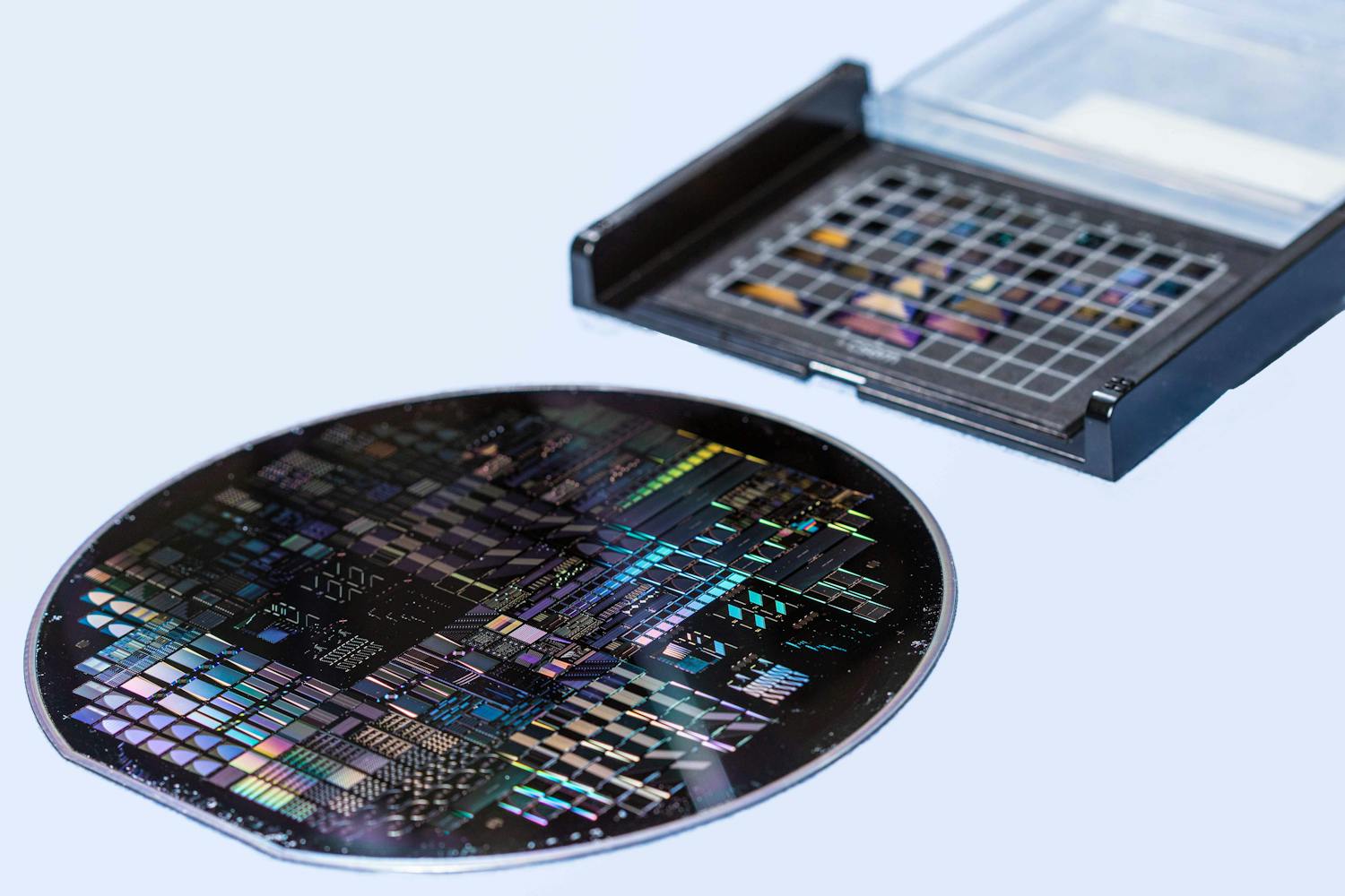
Photonic Integrated Circuits (PICs) manufactured in 150 mm wafer-scale process. © CSEM

CSEM was among the first to introduce an open-access foundry service for standardized TFLN PICs (Thin-Film Lithium Niobate on Insulator Photonic Integrated Circuits), designed specifically for prototyping, and research and development. The distinctive features of this service include a unique combination of three device layers, two metallization steps, cladding, back-end-of-line opening steps, and seamless chip facets integrated into a monolithic PIC platform.

This integration opens up a myriad of possibilities for intricate PIC designs, as well as hybrid and heterogeneous integration. Moreover, it facilitates easy electrical and packaging interfacing.

Our state-of-the-art technology and expertise in the PIC domain ensure superior quality and performance for applications in telecommunications, data centers, quantum, and beyond. Now is the time to partner with CSEM to leverage the potential of TFLN in your innovative projects.

Learn how Miraex leveraged our TFLN foundry services for breakthrough photonics solutions.

Process Design Kit (PDK) C-band building blocks

Process design kit for TFLN PICs

CSEM TFLN PIC foundry services is supported by a dependable process design kit (PDK) on telecommunication C-band. The PDK encompasses a set of active and passive building blocks, technology layers and design guide documentation.

Furthermore, CSEM provides the PIC designer with parametric cells (PCell) for the building blocks. This enables the designer to turn the standardized components into customized ones (in compliance with the fabrication design rules), easing the layouting and circuitry of the customized PICs.

CSEM’s PDK is now available at LUCEDA.

LUCEDA Photonics Logo
Multiple 5x5 mm² chips fabricated on CSEM's TFLN PIC platform.

Why work with us

  • MPW and custom RUNs (3-4 RUNs / year)
  • Extensive library of standardized building blocks
  • Expert check and consultation
  • Design rule check (DRC)
  • Design, simulation, layout, and characterization services
  • ISO9001-certified 150 mm wafer foundry
  • Independent and innovative foundry located in the heart of Europe
  • Confidentiality 
      

Current offerings for thin-film lithium niobate PICs

CSEM's TFLN PIC foundry service covers design, manufacturing, and testing needs.

Schedule of the MPW RUNs

We support a robust MPW life cycle by assisting photonic designers at every stage of mask preparation. This includes systematic DRC during design submission and functional-level consulting, as well as advice to optimize PIC designs.

Full stack MPW

null

Fast MPW

CSEM’s TFLN PIC fast MPW RUNs calendar

Take the next step in your photonics journey

Reach out to us for a consultation and discover how we can tailor solutions to meet your specific needs.

Check out our flagship EU projects!

Motivation for the next generation of Photonic integrated circuits

Frequently asked questions about TFLN PICs and access to the platform

Would you support us in the chip design?

Is it possible to have access to some demo test chips before placing an order for a service?

How long is the lead time for the MPW and dedicated RUN?

Do you provide flexible PCells on top of the standard PDK building blocks?

Do you have PDK at other wavelengths than C-band?

What is the cost of a dedicated RUN?

Meet our happy customers

Logo MIT

Mikkel Heuck

Forschungswissenschaftler Quantenphotonik-Labor

Wir unterstützen nachdrücklich die Bemühungen des CSEM, eine Wafer-Produktion für integrierte Lithiumniobat-Photonik aufzubauen, da wir glauben, dass dies sowohl für die Industrie als auch für die Wissenschaft von grosser Bedeutung sein wird. Wir schätzen uns glücklich, uns hier frühzeitig beteiligen und mit dem CSEM zu einem Zeitpunkt zusammenarbeiten zu können, da das CSEM seine Möglichkeiten ausbaut, wodurch wir unsere Forschung im Bereich der integrierten Quantenphotonik beschleunigen können.

Logo Eblana Photonics

Richard Phelan

Leiter Laserentwicklung

Wir haben mehrere Projekte mit dem CSEM abgewickelt, im Rahmen derer wir unsere Halbleiterlaserprodukte erheblich weiterentwickeln und uns neue kommerzielle Möglichkeiten im Bereich der Laser mit geringer Linienbreite für Lidar-Anwendungen eröffnen konnten. In intensiven Gesprächen mit den Spezialisten des CSEM gewannen wir viele neue Ideen und wertvolles Feedback für verschiedene Anwendungen wie Metrologie und Sensorik.

Logo Brolis Sensor Technology

Augustinas Vizbaras

Technischer Leiter

Das CSEM hat ein detailliertes Verständnis und fundiertes Wissen in der Verwendung optischer Systeme zur Messung von Vitalparametern. Wir konnten dieses Know-how auf unseren Anwendungsfall anwenden und so unsere OptiBP-Software und das globale Management des Bluthochdrucks entscheidend verbessern.